Abstract
Hafnium disulfide (HfS2) monolayer is one of the most promising two-dimensional (2D) materials for future nanoscale electronic devices, and patterning it into quasi-one-dimensional HfS2 nanoribbons (HfS2NRs) enables multi-channel architectures for field-effect transistors (FETs). Electronic, transport and ballistic device characteristics are studied for sub-7 nm-wide and ~15 nm-long zigzag HfS2NR FETs using non-equilibrium Green’s functions (NEGF) formalism with density functional theory (DFT) and maximally localized Wannier functions (MLWFs). We provide an in-depth analysis of quantum confinement effects on ON-state performance. We show that bandgap and hole transport mass are immune to downscaling effects, while the ON-state performance is boosted by up to 53% but only in n-type devices. Finally, we demonstrate that HfS2NR FETs can fulfill the industry requirements for future technology nodes, which makes them a promising solution for FET architectures based on multiple nanosheets or nanowires.
Keywords: density functional theory (DFT); hafnium disulfide (HfS2); nanoribbon; non-equilibrium Green’s function (NEGF); quantum transport; quasi-one-dimensional
1. Introduction
Atomically thin two-dimensional (2D) materials (2DMs) have arisen as potential candidates for future transistor channel materials [1,2,3] since the discovery of graphene in 2004 [4]. The 2DMs exhibit near-ballistic transport properties and show potential for future high-performance electronic devices due to atomic thickness and dangling-bond-free surfaces [5]. Despite their promising characteristics, the 2DM devices are severely limited by the high contact resistance that degrades the device performance [6,7,8]. After graphene, more than 1800 2DMs have been predicted to be stable [9], and many of them have shown promise as channel material with transition metal dichalcogenides (TMDs), such as MoS2, MoTe2, WS2, WSe2, SnS2, etc. [10,11,12], being among the most promising for future FETs. One hundred 2DMs were studied recently in [13] for future logic devices where monolayer hafnium disulfide (HfS2) is reported to be one of the best-performing 2DMs for future ultra-scaled FETs due to a combination of electronic and transport properties such as low effective mass and high injection velocity that result in high ON-state current for both n- and p-FETs. The electronic, transport, and device properties of 2D HfS2 were studied in detail in [13,14,15] by advanced theoretical calculations, whereas experimental work on few-layer HfS2 FETs was reported in [16,17] where integration compatibility of monolayer HfS2 with HfO2 high-k dielectric was emphasized as one the biggest strengths of realization of devices with HfS2.
With current state-of-the-art multi-bridge channel (MBC) FETs with silicon nanosheets or nanowires gaining momentum in the industry, 2DMs patterned into quasi-one-dimensional (quasi-1D) structures such as nanoribbons could replace silicon and extend Moore’s law by offering higher integration density [18,19,20]. Additionally, quantum confinement effects provide avenues for tuning the material properties, which could benefit the performance of such electronic nanodevices. Recently, various nanoribbons with ultimately downscaled widths were experimentally reported, including graphene nanoribbons (GNRs) [21,22] and phosphorene nanoribbons (PNRs) [23,24], which affirms the possibility of constructing MBC FETs, at least in principle, with quasi-1D 2DM nanostructures. Therefore, given the promising performance of 2D HfS2 FETs, it is imperative to systematically explore the electronic, transport, and device properties of quasi-1D nanoribbons of HfS2 (HfS2NRs) about which nothing is currently known in the literature.
In this paper, we present an ab initio study on HfS2NRs using density functional theory (DFT) to obtain the electronic structure, and maximally localized Wannier functions (MLWFs) to transform DFT Hamiltonians into localized basis suitable for quantum transport simulation. The MLWF Hamiltonians are then coupled to our in-house non-equilibrium Green’s function (NEGF)-based quantum transport [25,26] solver to obtain the relevant properties of HfS2NRs and HfS2NR FETs. Most importantly, we report the degradation of pFET performance while scaling down the nanoribbon width; however, the driving current in HfS2NR nFETs is surprisingly boosted in ~2 nm-wide transistors by the quantum confinement effects. These findings are further explained by investigating the bandgap, density of states and carriers, current density, and injection velocity. Finally, we compare HfS2NR n- and p-type FETs to other 2DMs and to the requirements set in the International Roadmap for Devices and Systems (IRDS). We show that both n- and p-type HfS2NR FETs with nanoribbon widths in the range from ≈2 nm to ≈5 nm can fulfil the goals set for future logic devices.
2. Methods
The unit cell of monolayer HfS2 (Figure 1a) is obtained from the Materials Cloud [27] and scaled to construct the supercells of zigzag HfS2 nanoribbons with hydrogen-passivated edges. The nanoribbon structure from the top and side views is shown in Figure 1b and Figure 1c, respectively. The zigzag direction exhibits the highest curvature of the dominant subbands in the valence and conduction bands, which hints at excellent carrier transport in these devices. The HfS2NR supercells are constructed with respect to the number of HfS2 unit cells repeated along the nanoribbon width (W). This number ranges from 2 to 10 unit cells, which corresponds to W from 1.36 nm to 6.39 nm. After defining the initial structure, we employ an ab initio plane-wave DFT, implemented in the Quantum Espresso (QE) program package (v.6.8) [28], to relax the nanoribbon structure and obtain the Hamiltonians. A 20 Å vacuum is added in confined directions to exclude any interactions between layers. The DFT calculations use Perdew–Burke–Ernzerhof generalized gradient approximation (PBE-GGA) [29] as the exchange–correlation functional with plane augmented wave (PAW) pseudopotentials. The Brillouin zone is sampled with 1 × 15 × 1 Monkhorst–Pack k-point grid [30] where 15 k-points are in transport direction, and the cutoff energy is set to 1360 eV. Convergence thresholds for ionic forces are fixed to 10–3 eV/Å, while 10–4 eV is used for total energy.

Figure 1. Illustration of (a) HfS2 monolayer. (b) Top and (c) side view of the monolayer HfS2 nanoribbon with zigzag edges. (d) Band structure obtained from DFT (blue dots) and MLWF (red lines).
Energy-localized plane-wave Hamiltonians from QE are then converted into a space-localized basis using MLWFs [31] implemented in the Wannier90 (v.3.1.0) program package [32,33]. The main input into the Wannier90 tool are the trial orbitals that are used for Wannier transformation, and here we use d orbitals for Hf atoms and p orbitals for S atoms. The band structure calculated with MLWF and DFT Hamiltonians shows good agreement in the relevant energy region around the bandgap, as seen in Figure 1d that reports the dispersion of the 3.25 nm wide HfS2NR. Finally, the supercell MLWF Hamiltonian matrices are upscaled to construct the total HfS2NR Hamiltonian, where the ~15 nm-long nanoribbon represents the channel of the HfS2NR FET.
Being primarily interested in the ON-state performance, we use the top-of-the-barrier (ToB) ballistic FET model [34] to simulate single gate n- and p-type FETs with HfS2NR channel. Within the ToB model, only the thermionic current is calculated, which is reasonable because the assumed 15 nm long channel is long enough for negligible tunnelling. The main inputs of the ToB FET model are transmission and density of states (DOS) calculated using the NEGF formalism implemented in our in-house code [35,36]. Within NEGF, the channel is described with the total HfS2NR Hamiltonian and source/drain (S/D) contacts are described with S/D self-energy matrices calculated using the numerically efficient Sancho–Rubio method [37,38]. The n- and p-type FETs with zigzag HfS2NR channels are simulated with ideal electrostatic control by the gate, resulting in a perfect subthreshold slope, equivalent oxide thickness (EOT) of 1 nm, S/D doping set at 0.01 areal molar fraction or ≈2.7 × 1013 cm−2, and supply voltage (VDD) set to 0.7 V. To provide a meaningful comparison between various HfS2NR devices, simulations are performed with a common OFF-state current (IOFF) set to 10 nA/μm as defined by IRDS for high performance (HP) devices [39].The setting of IOFF is performed by adjusting the gate work function for each device automatically within our code. The ballistic ON-state current (ION) and the ON-state charge density at ToB are extracted when both gate and drain are biased at the supply voltage. Finally, we set EOT to 0.6 nm and compare ION and injection velocity to our previous work on GeS nanoribbon devices, in addition to one hundred 2DMs reported in [13].
3. Results and Discussion
Band structure of HfS2NRs with various widths is reported in Figure 2a–d. All HfS2NRs exhibit a direct bandgap at the Γ point and we observe an immunity of bandgap (Eg) to width scaling. The bandgap keeps a constant value of ≈1 eV in all nanoribbons, as reported in Figure 2e, which is slightly smaller than the 1.3 eV reported in [13] for the HfS2 monolayer. As W is scaled down, the conduction band (CB) exhibits fewer bands near the CB minimum (CBM), while the dominant subband qualitatively remains the same. On the other hand, two degenerate subbands are visible in the valence band (VB) of wide HfS2NRs with W > 4 nm, and this degeneracy is broken in narrower nanoribbons due to strong quantum confinement effect. Namely, two-hole subbands separate and this separation increases with W downscaling, which is followed by an increase in the curvature of the second subband near the VB maximum (VBM). To further investigate the quantum confinement effects on the band structure of all HfS2NR widths, we extract the electron and hole–band structure effective mass of the dominant subband, closest to the CBM or VBM, from the band structure by fitting its curvature with a parabolic approximation (Figure 2f). Electron effective mass (me*) is immune to scaling with me* ≈ 0.2m0 for all nanoribbon widths. In contrast, hole effective mass (mh*) experiences a significant width-scaling effect. Namely, mh* is ≈0.37m0 for HfS2NRs with W ≥ 3.25 nm; while scaling down the width linearly decreases mh* to 0.33m0 when W = 1.36 nm. Considering only the observed differences in CB and VB, where the mh* of the dominant (highest) subband is at least 1.6 × lower than the me* for all observed HfS2NRs, we expect a considerable difference in the performance of n- and p-FETs with HfS2NR channels. However, this metric does not take into account degeneracy in VB or the higher number of subbands near CBM in wider nanoribbons.

Figure 2. Band structure of zigzag HfS2NRs with the widths of (a) 1.36 nm, (b) 1.99 nm, (c) 3.88 nm and (d) 6.39 nm. (e) Impact of nanoribbon width-scaling on the bandgap of zigzag HfS2NRs. (f) Electron and hole band structure effective mass dependence on nanoribbon width. Effective masses are extracted for the lowest (highest) subband in the CB (VB).
To assess the performance of n- and p-type HfS2NR FETs in Figure 3a, we plot the nanoribbon width dependence of the width-normalized ON-state current. The HfS2NR pFETs exhibit a monotonic ION decrease from 1.5 mA/μm to 1.12 mA/μm when the width is downscaled. The only exception is the narrowest pFET that shows a slight ION increase to 1.18 mA/μm. On the other hand, for HfS2NR nFETs, we surprisingly observe a generally monotonic increase of ION when HfS2NR width decreases. The ON-state performance is enhanced from 1.14 mA/μm to 1.74 mA/μm when the width is downscaled from 6.39 nm to 1.99 nm, whereas the narrowest nanoribbon with W = 1.36 nm exhibits a slight decrease of ION to 1.66 mA/μm. Therefore, quantum confinement effects induce a current boosting of 53% for nFETs with the ≈2 nm wide HfS2NR channel. Since the performance of HfS2NR FETs shows no correlation to the band structure effective mass, in the following paragraphs, we explore the features of charge density, density of states, and carrier injection velocity.

Figure 3. (a) ON-state current and (b) charge density at ToB width dependence in n- and p-type zigzag HfS2NR FETs. ION and Qch are extracted at VGS = VDS = VDD = 0.7 V with a common IOFF = 10 nA for all devices. Comparison of DOS in (c) conduction and (d) valence band of HfS2NR FETs. All DOS and transmission plots are shifted so that the CBM and VBM are positioned at 0 eV. Dependence of injection velocity on gate voltage in (e) n-type and (f) p-type zigzag HfS2NR FETs for various nanoribbon widths.
Charge density at the top-of-the-barrier extracted in the ON-state (QCH) for various HfS2NR widths is plotted in Figure 3b. For HfS2NR nFETs, we report QCH ≈ 8.3 × 1012 cm−2 for W ≥ 3.88 nm, while scaling down decreases QCH to 7.88 × 1012 cm−2 in the 1.36 nm wide device. On the other hand, in pFETs, charge density increases monotonically from QCH = 7.87 × 1012 cm−2 for W = 6.39 nm to QCH = 8.24 × 1012 cm−2 for W = 1.36 nm. Charge density at the top-of-the-barrier depends on DOS near the CBM or VBM. Therefore, we plot DOS near the CBM (VBM) for various HfS2NR widths in Figure 3c,d. The HfS2NR nFETs exhibit a dense DOS with a high number of Van Hove singularities (VHS) near the CBM. Scaling down, HfS2NR width reduces the number of available bands in the CB, decreases the overall DOS in the 100 meV window, and, therefore, lowers the charge density in narrower HfS2NRs. However, VB DOS that is relevant for HfS2NR pFETs shows an increase from a single VHS to two VHSs near the VBM due to band separation of the two dominant subbands (see Figure 2a) which increases the DOS near the VBM and QCH when nanoribbon width is scaled down.
Since the trends in ION and QCH behavior, reported in Figure 3a,b, are qualitatively opposite, the only reasonable explanation for ION trends should be found in the carrier transport properties, i.e., injection velocity. Injection velocity (vinj) represents the average carrier velocity at the top-of-the-barrier under the ballistic limit and it is shown in Figure 3e,f for n- and p-type HfS2NR FETs, i.e., electrons and holes, respectively. The plots report a gate voltage (VGS) dependence of vinj in the range from the threshold voltage (VGS ≈ 0.2 V) to the supply voltage (VGS = 0.7 V). The nFETs with W ≥ 5.14 nm show almost no modulation by VGS with electron vinj being ≈0.8 × 107 cm/s. In contrast, vinj increases with increasing bias in the 1.36 nm and 1.99 nm wide HfS2NR nFETs. These two devices exhibit similar vinj at the threshold voltage; however, HfS2NR nFETs with W = 1.99 nm exhibit a stronger bias modulation and a higher maximum electron vinj of 1.39 × 107 cm/s. The best observed vinj coincides with the best reported ION in nFETs for the 1.99 nm wide HfS2NR nFET. We attribute the optimum performance and highest electron vinj for W ≈ 2 nm to the band structure evolution, especially to the second CB subband visible in Figure 2b. Namely, for this nanoribbon, the subband crowding is not as dense as for wider HfS2NRs, which means that higher subbands with heavier carriers do not contribute significantly to the current-carrying process. As for pFETs, hole vinj at the threshold equals ≈ 0.8 × 107 cm/s for all HfS2NR pFETs. Scaling down, HfS2NR width decreases the strength of VGS modulation of the hole vinj, and devices with W ≤ 2.63 nm show almost no bias modulation. The widest observed HfS2NR (W = 6.39 nm) shows a 49% increase of hole vinj to 1.2 × 107 cm/s in the ON-state. As the width is downscaled, the hole vinj decreases monotonically, which agrees with the ION behavior reported in Figure 3a.
We further explore the current and transport properties in ultra-scaled HfS2NR nanodevices by analyzing the current energy density (Jde) in the ON-state. The Jde results are shown for n- and pFETs in Figure 4a and Figure 4b, respectively. In all devices, the current is mainly contained in the energy window up to ≈100 meV from the CBM/VBM. The nFETs exhibit Jde maximum at the CBM for the narrowest HfS2NR, but wider HfS2NRs exhibit a slight shift of the maximum by 20–30 meV, due to the higher number of occupied subbands. Namely, setting a common IOFF for all devices results in different S/D Fermi levels (EF) depending on device width, with a greater EF shift upward generally observed for wider HfS2NRs. Consequently, there are more current-carrying subbands, and the current density at the CBM is lower in wider HfS2NR nFETs. The 1.36 nm wide HfS2NR shows maximum current density near the CBM, with only a single dominant subband. In contrast, for W = 1.99 nm, the second subband carries current as well, with the second-subband current density surpassing that of the first subband above CBM + 90 meV, which leads to the maximum ION for the 2 nm wide device among all the studied HfS2NR nFETs.

Figure 4. Current energy density at ToB in the ON-state for HfS2NR (a) n-type and (b) p-type FETs with different nanoribbon channel widths.
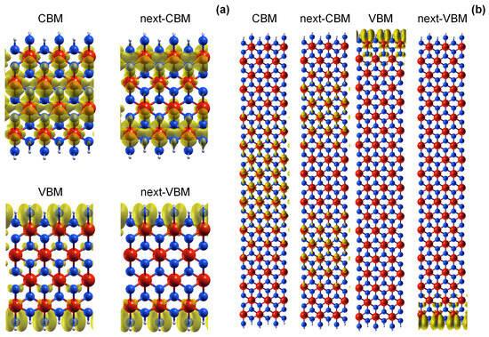
In addition to the current density, band decomposed charge density (BDCD) of nanoribbons with the widths of 1.36 nm and 6.39 nm is plotted in Figure 5a and Figure 5b, respectively. The BDCD is shown for subbands at the CBM/VBM, along with the nearest next subbands that are denoted as next-CBM/next-VBM. Figure 5a shows that the electron current in the narrowest nanoribbon, mainly determined by the first CB subband (see Figure 4a), is distributed almost through the whole nanoribbon width, except for edge S atoms. On the other hand, electron current in the widest HfS2NR is mostly determined by the next-CBM subband (see Figure 4a), so that the current flows away from the edges and somewhat through the middle, as shown in Figure 5b. As for HfS2NR pFETs with current density reported in Figure 4b, Jde is localized near the VBM due to the dominant first subband in the VB with a considerable contribution of the second subband in some devices. The lowest two VB subbands are slightly separated, i.e., degeneracy is broken, only in the narrowest HfS2NR (see Figure 2a), and this split results in lower transmission probability near the VBM and, therefore, lower Jde in pFETs with the narrowest 1.36 nm wide channel. As shown in the BDCD plots in Figure 5a,b, now addressing the situation for the VBM subband, we observe that the hole current is expected to flow exclusively along nanoribbon edges. Furthermore, for wide HfS2NRs where two degenerate subbands are dominant near the VBM, we observe that the current flows through separate edges in VBM and next-VBM, as seen in Figure 5b, due to zero overlap between the edges. Scaling down the nanoribbon width decreases the distance between the edges, which increases the overlap of the edge states and, therefore, causes the separation of degenerate subbands near the VBM, as seen in Figure 2. Increasing the current by increasing the width would be limited due to edge transport; hence, the narrowest HfS2NR pFETs exhibit a decreasing drive current (Figure 3a) due to higher DOS in S/D regions and related EF downshift.

Figure 5. Band-decomposed charge density of CBM, next-CBM, VBM and next-VBM subbands of (a) 1.39 nm and (b) 6.39 nm wide HfS2NRs. Isovalue is set at 0.001 q/bohr3.
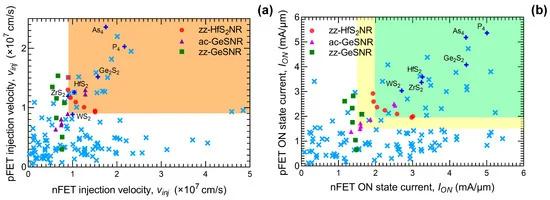
Finally, we compare the ON-state performance of HfS2NR FETs with one hundred 2DMs analyzed in [13], to the armchair and zigzag GeSNRs from our previous work [36,40], and to the IRDS requirements for future logic nodes [39]. For a proper comparison with the literature data, we set the EOT to 0.6 nm (HfO2 with εr = 20, tox = 3 nm) as in [13]. The injection velocity in the ON-state for nFET and pFETs is shown in Figure 6a. All HfS2NR n- and pFETs exhibit vinj close to, or higher, than the IRDS requirement (0.9 × 107 cm/s), while achieving comparable vinj values to those in 2D HfS2 along the zigzag direction. Furthermore, only a few other large-area 2D materials such as Ge2S2, As4 and P4 exhibit higher vinj compared to HfS2NRs. This is noteworthy because HfS2NRs are quasi-1D nanostructures with additional quantum confinement in comparison to 2DMs that are infinite 2D sheets.

Figure 6. (a) nFET vs. pFET ON-state injection velocity with orange area denoting injection velocity higher than 0.9 × 107 cm/s set by IRDS 2022 for future logic nodes. (b) nFET vs. pFET ON-state current with a green area representing IRDS 2021 maximum ION requirement with ION = 1.979 mA/µm, and a yellow area representing the minimum ION requirement for future logic devices with ION = 1.504 mA/µm. The 100 2DMs reported in [13] are included in graphs with the most relevant materials named directly and denoted with blue plus signs, while the unnamed 2DMs are presented with light blue crosses.
4. Conclusions


